How to make a speckle pattern suitable for Digital Image Correlation?
- By Floriane Soulas, R&D engineer at EikoSim
Context: Speckle patterns & digital image correlation
The principle of image correlation is based on tracking information from a so-called “reference” image in the following images, often called “deformed images.”
When using digital image correlation (DIC), speckle patterns are created on the surface of a specimen to address uniqueness concerns. As a result, the accuracy of image correlation is heavily influenced by the speckle patterns.
All of the images form a film from which we seek to extract a measure.
We can therefore see the correlation of images as following points over the entire observed surface: following the movements of a part’s surface is equivalent to following the movements of all the points of this surface.
This requires the part to be “textured”: if there is only one black point, we cannot measure the displacement and the deformation of the white zone surrounding it.
For a point to be recognized, you need a that allows you to recognize the area around the point of interest. This texture is called a speckle pattern.
What is a speckle pattern?
A speckle pattern is created when multiple wavefronts with varying phases interfere with each other, resulting in a random intensity pattern. The amplitude and intensity of the resultant wave also vary randomly.
Most of the time, speckles are sprayed.
We just spray spots of black mat paint, of random sizes, on a white background and also a mat to avoid reflections that could interfere with the measurement.
A speckle of white dots on a black background is also possible.
To achieve spot sizes of the order of ten microns, it is possible to use an airbrush, as explained in the article about image correlation for lattice structures.
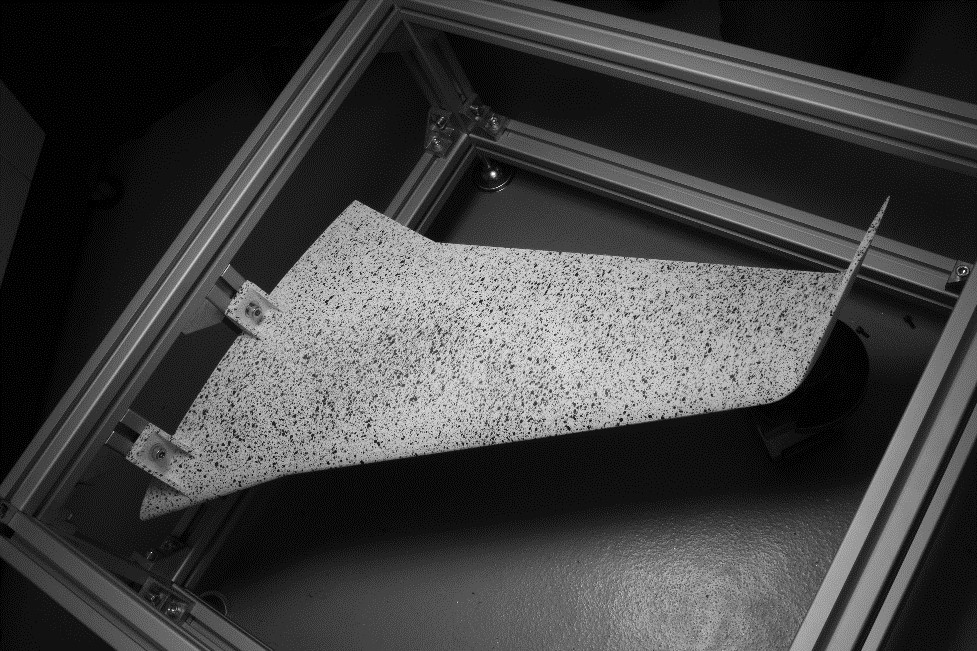
Fig.1 – Example of speckle pattern on airplane wing model.
What is a “good speckle pattern”?
To make a good speckle pattern, it must be:
- Random
- With spot sizes adapted to the measurement carried out.
To check that the speckle pattern is random and does not contain too much black or too much white, we can use grey-level histograms.
An optimal histogram is a “flat” one with an equivalent distribution of white and black.
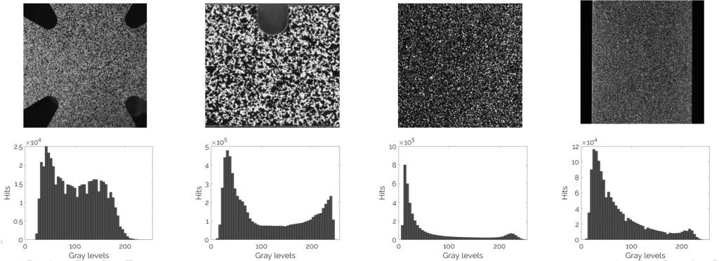
Fig.2 – Example of grayscale histograms for different types of speckle patterns
It is also necessary to take care to adapt the size of the spots.
This results from a compromise between the phenomenon studied (fine spots) and the image’s resolution (size large enough to be visible by the sensor).
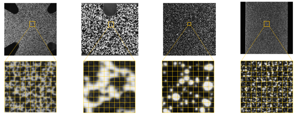
Fig.3 – Compromise speckle size/sensor resolution
Speckle pattern using spray paint
Tutorial: Making a Speckle Pattern
Different types of speckles encountered during EikoSim’s tests
It is sometimes possible to do without the speckle pattern step.
Indeed, certain materials, such as concrete, even have a “natural” texture that has sufficient heterogeneity to act as a natural speckle pattern, as shown in Fig. 4.
With this type of surface, it is possible to directly process the images without painting the structure.

Fig.4 – Example of a concrete surface with a “natural” speckle pattern
For the cases where one wishes to study displacements of the rigid body only (the shortest distance between the starting and ending position of a moving rigid body), without deformation, it is possible to create a speckle pattern digitally and print it on adhesive sheets, which will be deposited on the structure to be studied.
The advantage of this technique is that the randomness, as well as the management of the size of the spots, are entirely controlled by the user, who can choose for themselves the min and max diameters of his speckle spots.
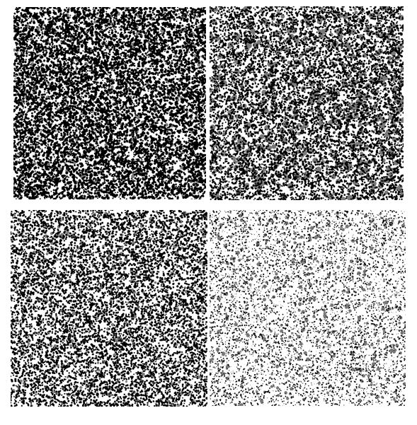
Fig.5 – Example of digitally generated speckle patterns with different sizes and number of spot criteria
Finally, there are still other speckle pattern methods, like the one developed by ALPhANOV
written and illustrated by Girolamo MINCUZZI and Simon NOURRY
It is well known that after irradiating the surface of a material like metal, semiconductor or even transparent dielectric with few ultrashort pulses, it is possible to modify the surface morphology with the generation of subwavelength ripples.
These ripples are perpendicular to the polarization direction and are referred as LIPSS: laser-induced periodic surface structures (see Fig.6 (a) and (b)).
By increasing the number N of pulses, LIPSS tends to be transformed in micro-grooves that are parallel to the polarization direction (see Fig.6 (c) and (d)).
Finally, by further increasing N, speckle pattern spikes with a characteristic size of ≈10 µm appear on the surface (see Fig.6 (e) and (f)).
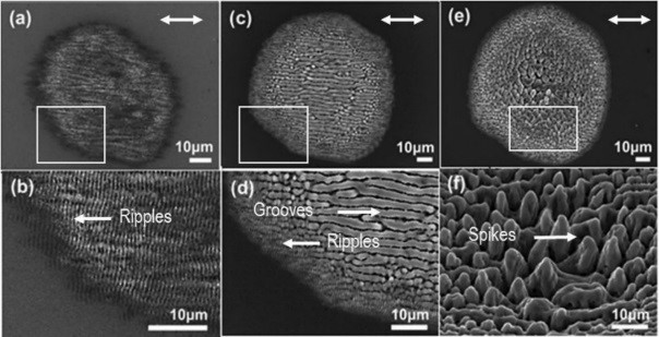
Fig.6 –Speckle pattern evolution of Si surface morphology upon irradiation of fs laser. 1(a) and 1(b) shows ripples, 1(c) and 1(d) micro grooves, 1(e) and 1(f) spikes
Thanks to these surface structures, it is possible to control the surface reflectivity R over a wide range of values.
Interestingly, in the case of surfaces covered with spikes, light experiences multiple reflections enabling a light trapping mechanism reducing R < 10%.
This effect is enhanced when the speckle pattern spikes surface consists of nanometric pores.
In the last case (see Fig.7 left), values of R < 5% can be obtained, yielding a “deep black” effect (see Fig.7 right).
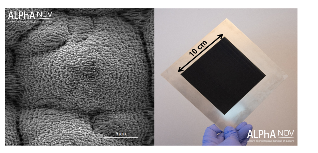
Fig.7 – (Left) Speckle pattern spikes with the porous surface on stainless steel, (right) a 10cm x 10cm stainless steel, deep black (R = 4%) surface
Moreover, thanks to the synchronized use of laser beam scanners and translation stages it is possible to efficiently process surfaces larger than a single pulse spot and varying from some tens of microns up to nearly 1m.
Here we carried out a preliminary, systematic investigation of how process parameters like, scan speed, hatch, number of successive scans, and pulse energy will impact the morphology and the R-value of a mirror-like, stainless-steel surface.
For all tests, we used a 350-fs pulsed laser emitting at λ = 1030 nm with a repetition rate of 500 kHz (Tangerine from Amplitude Systemes) and spot size 2ω0 ≈ 35 µm. Values of R ≈ 20% corresponding to a grey color were found for surfaces having a size comprised between 1cm2 and 0.2mm × 0.2mm utilizing the same set of process parameters.
On the contrary, for R< 5%, we observed that the size of the processed surface has a huge bearing on the final result.
For instance, Fig.8 shows the case of two similar surface morphologies and colors (R<4%).
But, whilst Fig.8 left is relative to a 1cm2 and has been processed with a pulse energy of E = 50 µJ, Fig.3 right is relative to 100µm × 200µm and has been processed with E = 32 µJ.
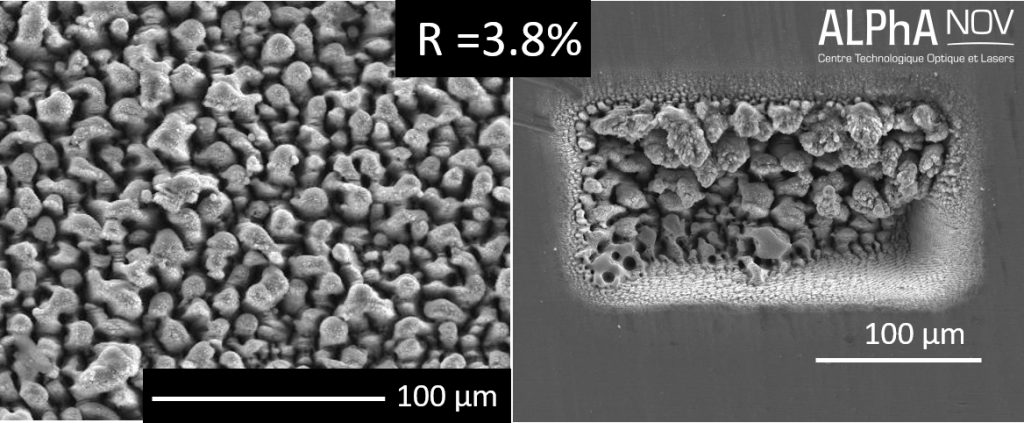
Fig.8 – Speckle pattern surface morphology of stainless steel enabling R<4%. Surfaces with two different sizes were processed: 1cm2 (left) and 0.1×0.2 mm2 (right)
Finally, we utilised all the results obtained from this preliminary investigation to process a surface of 10cm × 10cm.
We made two different patterns having features with different sizes and varying from some cm2 to ≈100 µm×100 µm. Results are shown in Fig. 9.
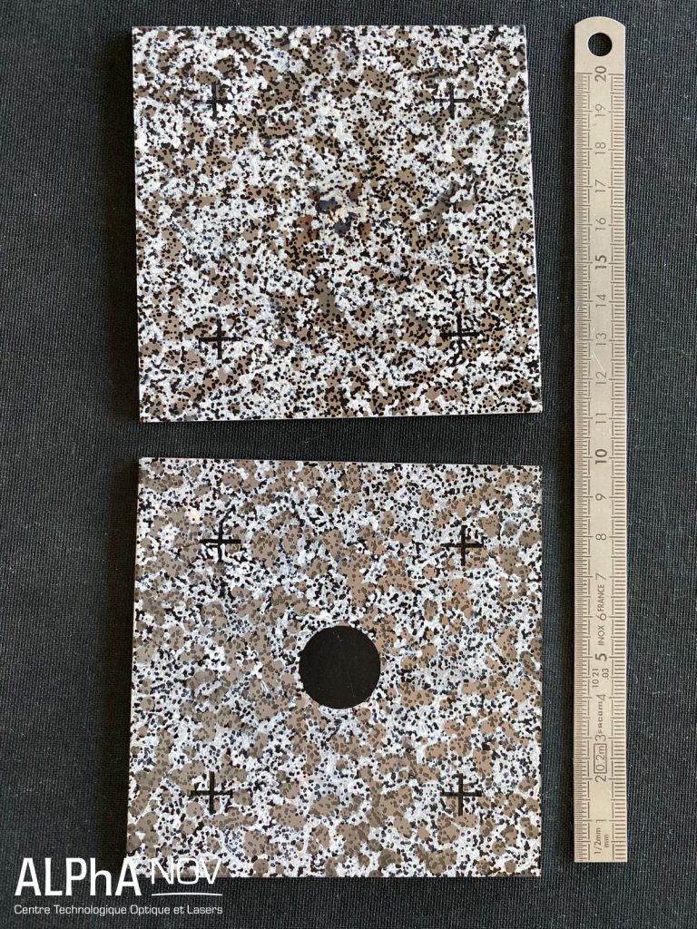
Fig.9 – Final “multi-colour” patterns made by fs laser over 10 × 10 cm2 stainless steel surface
We were finally able to create a speckle pattern with different levels of grey (by mixing the random creation of white, grey, and black) on a mirrored steel surface.
This specific speckle pattern was then used in a stereo-correlation study in collaboration with EikoSim.
98-100 AVENUE ARISTIDE BRIAND
92120 MONTROUGE
FRANCE